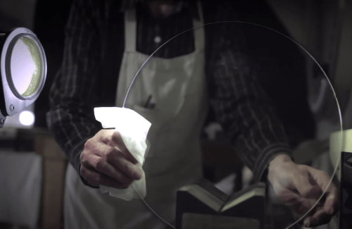
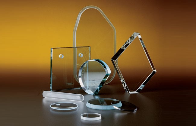
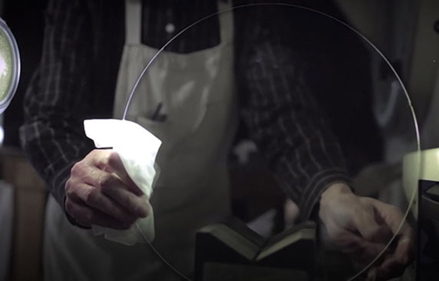
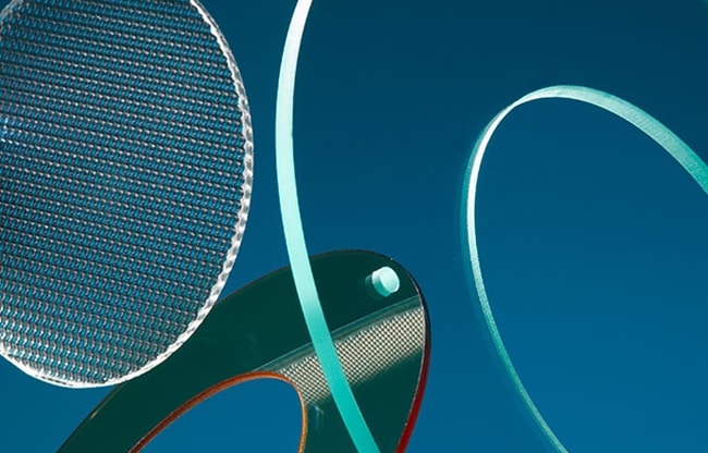
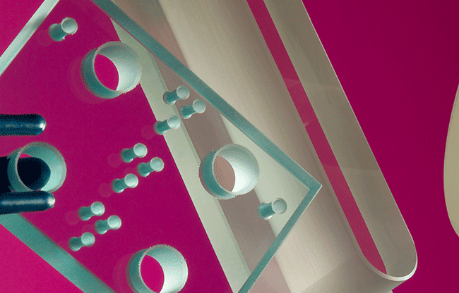
At Swift Glass, we’ve honed our glass design and production capabilities for more than 80 years. Using the latest innovations in glass manufacturing technology, we can fabricate a wide range of high quality standard or custom-designed glass wafers to suit the needs of many applications.
When you bring your glass wafer production project to Swift Glass, you’ll gain access to the highest quality materials, the most advanced cutting tools and finishing machines, and one of the most experienced teams in the industry.
Glass Wafer Applications & Industries
Glass wafers are used in a wide variety of technical and industrial applications. Some of these applications include:
Microelectromechanical systems (MEMS) and Electronics
In MEMS applications, glass wafers are often used as a substrate carrier in the fabrication process for thinner silicon wafers. MEMS components such as silicon wafers have broad applications in micro sensor, electronics, and computer manufacturing.
Semiconductors
Glass wafer and silica wafer usage in semiconductor manufacturing varies based on design. Glass wafers may be used as a permanent substrate which remains in the final product or as a temporary substrate for smaller or thinner materials.
Biotechnology
Scientists and researchers increasingly use glass wafers to fabricate microfluidic chips. Borosilicate chips can be particularly useful for these applications because of their affordability and high chemical resistance.
Integrated circuit (IC) packaging
Rather than cut individual circuits out of glass substrate, some manufacturers now leave them embedded within the wafer for protection. Durable wafer-level packaged ICs are becoming more common in portable electronics such as tablets and smart phones.
Our Glass Wafer Fabrication Process
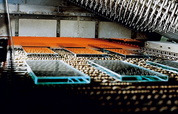
Glass wafer fabrication is a highly intricate process that requires specialized equipment and manufacturing procedures. To that end, our team of experts uses the most advanced technology available to create wafers that meet precise design standards. Our wafer fabrication process consists of several steps:
- Material Selection: We’ll work with you to determine the correct material for your design and use the most consistent sheet of glass available to cut flawless wafers.
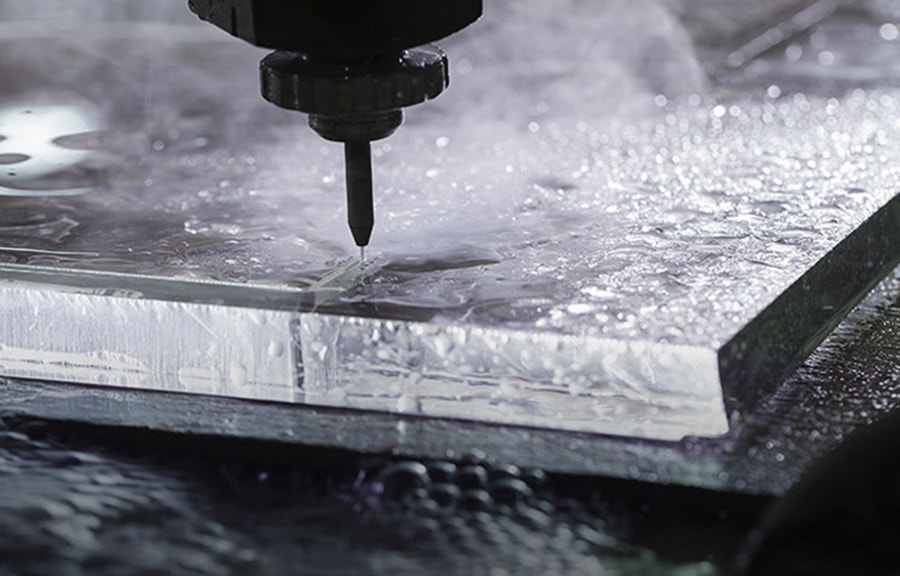
- Shaping: Once the selected material is cut with our advanced waterjet glass cutting tools, each wafer is ground into an approximate wafer shape.
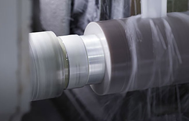
- Edging/Detailing: Our glass wafer fabrication process uses carefully calibrated CNC diamond machine tools, and each wafer is delicately machined to design specifications.
- Lapping and Polishing: We use a free abrasive lapping process to develop appropriate surface smoothness before polishing each wafer on both sides.
- Inspecting: Wafers undergo a high-precision laser inspection in a cleanroom to ensure that they fall within total thickness verification (TTV) standards.
Materials Used in the Glass Wafer Fabrication Process
Swift Glass begins our glass wafer fabrication process with only the highest quality glass materials. Which type of material we use depends on the requirements of the particular design.
The following materials are available for glass wafer fabrication:
- Borosilicate: Widely known as one of the most affordable glass fabrication materials, borosilicate glass retains its strength and transparency during exposure to high temperatures. A variety of borosilicate brands are available through Swift Glass from well-known manufacturers such as Schott and Corning.
- Borofloat ®: One of the most popular brands for glass wafer fabrication, this floating borosilicate glass material is renowned for its durability when exposed to corrosive chemicals, its impressive mechanical strength, and remarkable transparency.
- Quartz/Fused Silica: Quartz material is exceptionally pure and has an impressively high melting point. Fused silica wafers – also known as fused quartz wafers – are often considered ideal for use in semiconductor components due to their thermal shock resistance, near-zero thermal expansion rate, and ultraviolet transparency.
- Eagle XG ®: This glass material is created without many of the harmful chemicals traditionally found in electronic/computer components such as arsenic, halides, barium, or antimony. High chemical resistance, low density, and pristine clarity are all distinguishing characteristics of this material.
Glass Wafer Specifications and Customizations
Our high-tech two- and three-axis CNC equipment can cut and edge to nearly any specification. It’s also compatible with all of the most common file types:
With a specialty production shop and a prototype shop at our disposal, we can handle both low and high production runs—in fact, our minimum production run size is one unit. Our advanced waterjet cutting tools can cut your chosen material to wafer thicknesses down to 0.1 mm, and we can scale operations based on your specific glass wafer fabrication needs.
We also offer fully customized glass wafer fabrication. Our experienced team will not just help you fabricate your custom design—they’ll help you perfect it. We pride ourselves on our ability to take on designs and projects of any size.
We provide flexibility in our glass wafer offerings of thickness, flatness, surface quality, and edge profile. Examples of our specification range are as follows:
| For diameter measurements <200 mm | For diameter measurements >200mm | For Diameter measurements: >200mm but <450mm | |
|---|---|---|---|
| Thickness: | .3mm | .3mm to 10mm | .55mm to 10mm |
| Capabilities: | +/- 25µm | +/- 25µm | +/- 25µm |
| Total Thickness Variation (TTV): | <3µm | <3µm | <3µm |
| Surface Roughness (Root Mean Square) Average: | <12Â | <12Â | <12Â |
| Scratch Dig: | 40/20 | 40/20 | 40/20 |
| Bow: | <58µm | <58µm | <58µm |
| Warp: | <10µm | <10µm | <10µm |
| Flatness: | <1µm |
While our glass wafer and substrate fabrication services are most commonly used to create glass wafers and silica wafers for the MEMS and semiconductor sectors, our fully customizable processes and design can handle wafer fabrication for many industries and applications.
Glass Wafer Fabrication Experts
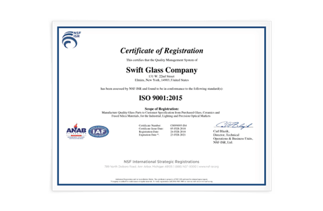
In over 80 years in glass fabrication, Swift Glass has witnessed the rise of many of the technologies that depend on glass and silica wafers. We proudly participated in the development of many of them. With such extensive experience, there’s no project that our knowledgeable team can’t handle. We’re also ISO 9001:2015 and ITAR certified, so you can be sure that when you choose Swift Glass, our processes and product quality will be second to none.
To learn more about glass wafer fabrication or our other services and products, contact us or request a quote today.
Click on the table below to learn more about our specifications.


