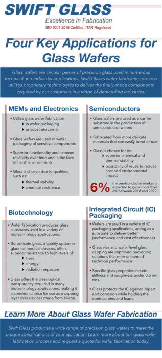
Four Key Applications for Glass Wafers
Leave a CommentGlass wafers are circular pieces of precision glass used in numerous technical and industrial applications. Swift Glass’s wafer fabrication process utilizes proprietary technologies to deliver the finely-made components required by our customers in a range of demanding industries.
High-quality glass material is selected, then the wafer is carefully shaped via cutting and grinding processes, then further machined to create the wafer’s edge profile and detailing, followed by finishing processes such as lapping and polishing. Each wafer is subjected to a highly controlled inspection process using precision laser measuring equipment to gauge total thickness variation and ensure it is within accepted tolerances.
Below, learn how glass wafer technology is being utilized in four popular sectors: MEMs and electronics, semiconductors, biotechnology, and integrated circuit (IC) packaging.
MEMs and Electronics
The microelectronic mechanical systems (MEMS) and electronics industries utilize glass wafer fabrication in wafer packaging and as substrate carriers. In MEMS and electronics applications, glass wafers are used in wafer packaging of sensitive components, due to their superior functionality and extreme reliability over time and in the face of harsh environments.
As a carrier substrate, glass is chosen due to qualities such as thermal stability and chemical resistance. In the medical device industry, these wafers are used to facilitate gas-tight MEMS enclosures.
Semiconductors
Glass wafers are used as a carrier substrate in the production of semiconductor wafers, which are fabricated from more delicate materials that can easily bend or tear. The glass substrate component allows the semiconductor wafer to be handled safely in spite of its delicate, thin qualities. Glass is chosen for its superior chemical and thermal stability, and the possibility of reuse can reduce cost and environmental impacts for some applications.
As the Internet of Things (IoT) continues to expand rapidly, the glass wafer semiconductor market is expected to grow more than six percent between 2018 to 2022. There is significant crossover between semiconductors and other sectors. For example, semiconductors (and the wafers they contain) are used in a variety of MEMS and consumer electronics featuring IoT connectivity.
 Biotechnology
Wafer fabrication produces glass substrates used in a variety of biotechnology applications. Borosilicate glass, a quality option in glass for medical devices, offers superior resistance to high levels of heat and energy, as well as radiation exposure, such as within X-ray equipment.
Wafers are also used in the production of microfluidic chips using nanoimprint lithography, where glass acts as a substrate. Glass offers the clear optical transparency required in many biotechnology applications, making it a common choice for use as a capping layer over devices made from silicon. Wafer bonding processes such as anodic and thermal bonding create a hermetic seal.
Integrated Circuit (IC) Packaging
Glass wafers are used in a variety of integrated circuit (IC) packaging applications, acting as a substrate to deliver better performance and cost effectiveness. Glass vias (TGV) and wafer level glass capping (WLC) are improved packaging solutions that offer enhanced technical performance, thanks to specific glass properties including stiffness and roughness under 0.5 nm rms. Glass protects the IC against impact and corrosion while holding the contract pins and leads that connect it to external circuits.
Learn More About Glass Wafer Fabrication
Swift Glass produces a wide range of precision glass wafers to meet the unique specifications of your application. Learn more about our glass wafer fabrication process and request a quote for wafer fabrication today.


 Advances in manufacturing technology have led to advances in glass shaping capabilities. Processes like state-of-the-art glass drilling,
  There are many different forms of edgework that you could specify for your glass part, and they all have an impact on the price of glass.
 Strengthening and tempering


